
How Alumina, Silicon Carbide and Aluminum Nitride support next-generation wafer processing
Advanced ceramics have become a core engineering requirement for semiconductor equipment manufacturers that need stable performance in extreme process conditions. As semiconductor process nodes move toward 2 nm and AI architectures drive higher thermal demands, ceramic components must withstand plasma exposure, harsh chemicals, high vacuum and rapid thermal cycling while maintaining tight dimensional control.
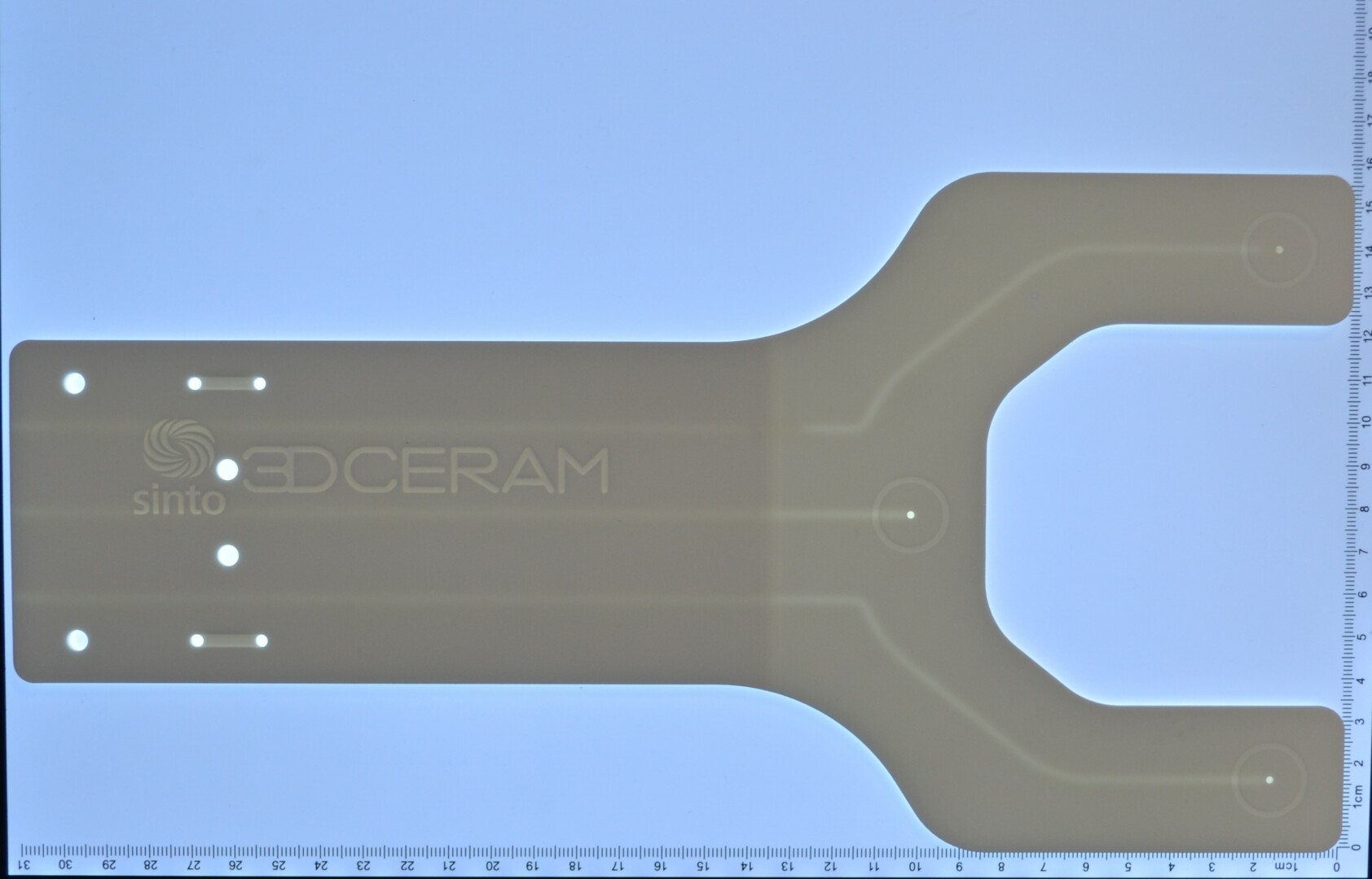
Standard industrial materials can degrade, contaminate process chambers or lose dimensional stability under the combined stresses of modern wafer processing. Advanced technical ceramics provide the electrical insulation, chemical resistance, mechanical rigidity and thermal performance required by front-end fabrication equipment. These requirements also apply to ceramic end effectors, the robot blades used to transfer wafers between process chambers, cassettes and handling stations.
For process engineers and fab equipment OEMs, material selection is therefore more than a supply chain decision. It is a design constraint that affects chamber cleanliness, wafer uniformity, component lifetime and the ability to qualify equipment for increasingly demanding process windows.
The surge in capital expenditure (capex) for new fabrication facilities, particularly for AI chips and advanced nodes, is directly driving the consumption of semiconductor-grade ceramics. Every new fab adds demand for process chamber components, wafer handling parts, thermal management elements and replacement consumables.
According to Dataintelo, the global semiconductor ceramic fabricated parts market is valued at $9.4 billion in 2025 and is projected to nearly double, reaching $18.7 billion by 2034. This expansion represents a compound annual growth rate (CAGR) of 7.9% from 2026 to 2034.
Growth is heavily concentrated in wafer processing applications, which accounted for the highest revenue share, at 34.2%, in 2025. As foundries invest in extreme ultraviolet (EUV) lithography, advanced packaging and higher wafer throughput, demand for reliable liners, rings, plates and thermal management components scales with the installed equipment base.
The performance of vacuum components, electrostatic chucks (ESCs) and process chamber interiors relies primarily on three technical ceramics: Alumina, Silicon Carbide and Aluminum Nitride. Each material occupies a different position in the engineering trade-off between electrical behavior, thermal transport, chemical resistance, machinability and cost.
| Material | Key strengths | Typical semiconductor applications | Main engineering trade-off |
|---|---|---|---|
| Alumina (Al₂O₃) | High-purity electrical insulation, rigidity, plasma resistance and mature supply chain. | Chamber liners, end-effectors, lifting pins, focus rings, gas distribution plates and structural insulators. | Reliable and cost-effective, but lower thermal conductivity than SiC or AlN. |
| Silicon Carbide (SiC) | Very high hardness, thermal stability, thermal conductivity and resistance to thermal shock. | Epitaxy and CVD components, susceptors and high-temperature process hardware. | Grade selection and finishing are critical; machining is demanding and electrical behavior varies by grade. |
| Aluminum Nitride (AlN) | High thermal conductivity combined with strong electrical insulation and a CTE close to silicon. | Electrostatic chucks, wafer handling, heat sinks and high-power packaging. | Excellent thermal performance, but cooling channels and tight geometries require precise engineering. |
Holding the largest material type share at 38.5% of the global semiconductor ceramic fabricated parts market in 2025, high-purity Alumina is the baseline standard for semiconductor tooling. It offers excellent dielectric strength, high mechanical rigidity and strong plasma resistance, which makes it suitable for insulating and structural parts exposed to demanding process chemistries.
Applications: In semiconductor manufacturing, alumina was used to produce customized lifting pins for CVD chambers, achieving full production qualification and enabling 600 validated sets to be delivered within weeks instead of months.
Silicon Carbide represents the fastest-growing segment in this space, with a projected CAGR of 9.4% through 2034. Its exceptional hardness, extremely high thermal conductivity and near-perfect resistance to thermal shock make it valuable for high-temperature processes where dimensional stability and service life are critical.
Applications: Silicon Carbide is essential for high-temperature processes such as epitaxy growth and chemical vapor deposition (CVD), as well as other environments where the component must resist aggressive plasma and repeated thermal cycling.
Engineering Note: SiC’s low coefficient of thermal expansion helps limit thermally induced stress and maintain dimensional stability during rapid thermal processing, although the exact behavior depends on the SiC grade, wafer material and process temperature.
As thermal budgets tighten, particularly for AI accelerator chips, Aluminum Nitride has become indispensable. Its ability to provide exceptionally high thermal conductivity, often exceeding 170 W/mK, while acting as a strong electrical insulator makes it a strong fit for heat-sensitive wafer handling and packaging systems.
Applications: Aluminum Nitride is the dominant material for electrostatic chucks (ESCs), high-power semiconductor packaging and specialized heat sinks. The key insight is the trade-off between electrical resistivity and thermal conductivity: AlN reaches a practical balance for modern wafer handling, while its internal cooling channels still require precise engineering and machining.
Historically, ceramic components were manufactured through dry pressing, extrusion or slip casting, followed by green machining and high-temperature sintering. These methods remain effective for established geometries, but they become less flexible when next-generation semiconductor equipment requires internal channels, thin sections or integrated functions.
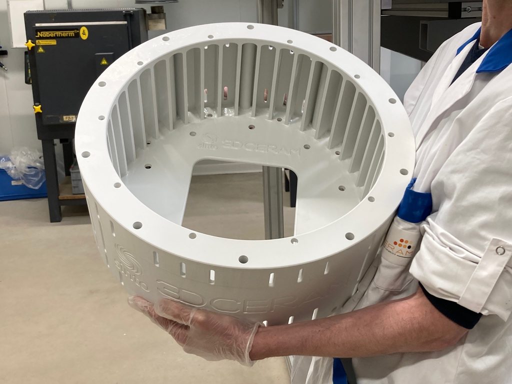
Machining technical ceramics is slow, expensive and restrictive when the component contains curved internal voids or complex surfaces. Stereolithography (SLA / VPP) ceramic 3D printing addresses this limitation by building the green part layer by layer from a digital model, followed by debinding and sintering.
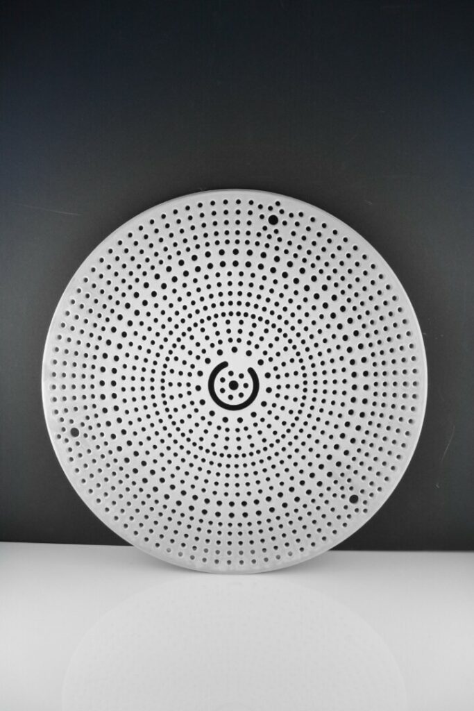
The most significant limitation of traditional machining is the inability to create complex, curved internal voids. In advanced ESCs and showerheads, uniform gas distribution and fluid cooling are critical. Ceramic 3D printing enables the fabrication of conformal cooling channels, internal pathways that closely follow the contours of the component. This can support more uniform thermal dissipation across a 300mm wafer, helping to reduce edge defects and protect yield. The same design logic can benefit lightweight ceramic end effectors, where rigidity, low deflection, thermal stability and particle control are essential during robotic wafer transfer.
Traditional assemblies often require joining multiple ceramic parts with brazing or mechanical fasteners, introducing potential leak points, dead zones and particle generation risks. Additive manufacturing allows 3DCeram Sinto to consolidate complex multi-part assemblies into single, monolithic structures. This level of functional integration can support cleaner operation in ultra-high vacuum (UHV) environments and extend component lifespan.
Engineering Note: Features such as diamond-inspired periodic open-cell structures, which maximize surface area for thermal or chemical reactions, cannot be machined in the same way as conventional forms. They must be grown layer by layer, making additive manufacturing a practical route to geometries that combine several functions in one ceramic component.
Fab equipment OEMs operate under demanding R&D timelines. Iterating a ceramic part conventionally can require expensive diamond-tooled molds and months of lead time. 3D printing eliminates the need for dedicated tooling, allowing engineers to move from a CAD file to a sintered, high-purity ceramic prototype in weeks and to iterate chamber liners, focus rings or custom wafer handling fixtures more quickly.
Meeting the demands of tomorrow's semiconductor fabs requires more than sourcing bulk material; it requires co-engineering geometries that push the boundaries of process performance. Material purity, print resolution, shrinkage compensation, debinding, sintering and finishing all contribute to the final component's behavior.
3DCeram Sinto provides stereolithography (SLA) ceramic 3D printing tailored explicitly for the semiconductor industry. By leveraging high-purity Alumina, Aluminum Nitride and Silicon Carbide, the engineering team helps OEMs pursue the thermal uniformity, plasma resistance and geometrical complexity required for sub-2nm nodes.
Advanced ceramics connect the electrical, thermal and chemical requirements of modern semiconductor fabrication. Alumina remains the dependable industry workhorse, Silicon Carbide serves the most thermally demanding environments and Aluminum Nitride provides a valuable balance of thermal conductivity and electrical insulation.
The adoption of ceramic 3D printing extends this material platform into more complex component designs. By enabling conformal cooling, monolithic integration and faster design iteration, additive manufacturing gives equipment engineers a practical route to improve performance while reducing tooling constraints.